|
China PCB Prototype Board Online Market
|
Gold Index: 12474


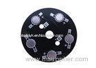
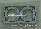
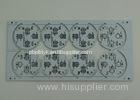
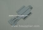
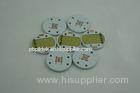
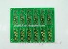
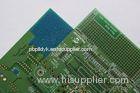
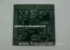
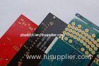
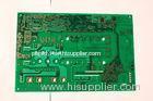
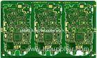
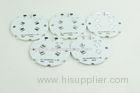
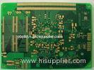
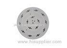
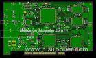
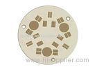
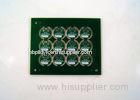
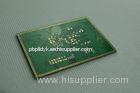
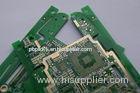
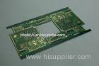
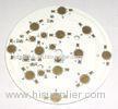
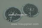
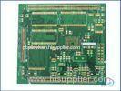
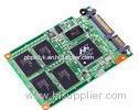
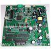
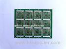
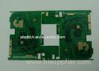
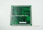
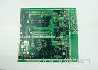
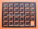
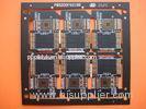
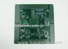
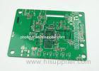
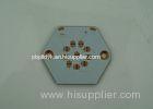
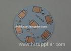
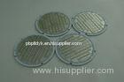
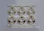
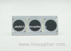
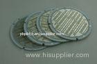
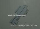
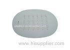
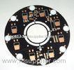
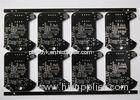
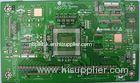
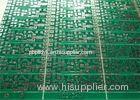
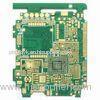
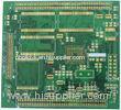
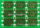
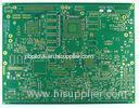
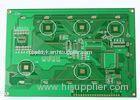
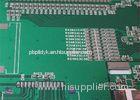
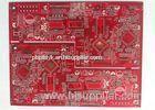
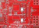
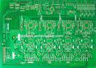
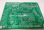
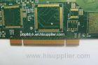
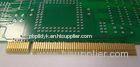
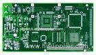
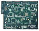
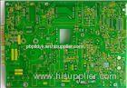
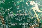
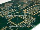
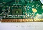
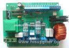
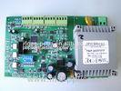
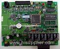
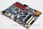
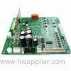
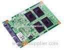
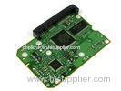
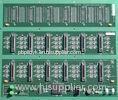
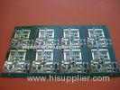
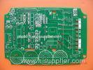
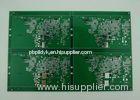
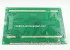
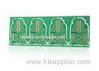
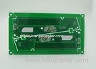
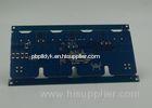
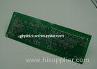
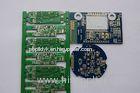
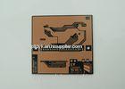
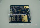
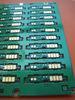
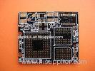
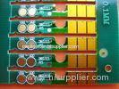
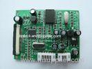
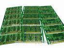
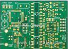
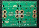
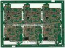
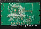
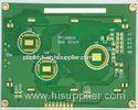
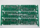
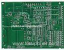
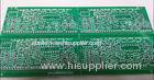
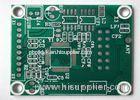
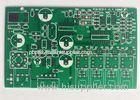
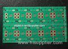
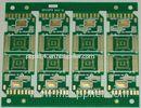
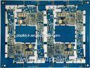
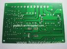
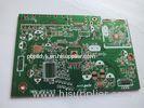
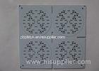
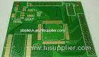
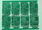
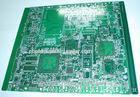
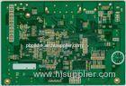
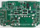
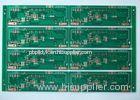
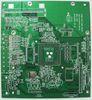
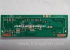
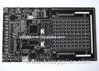
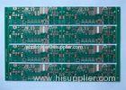
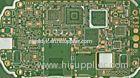
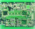
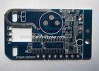
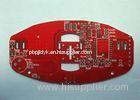
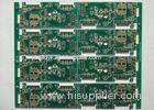
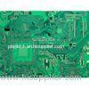
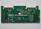
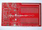
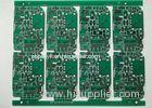
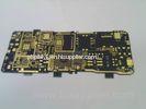
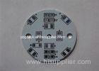
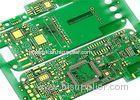
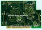
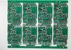
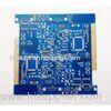
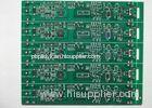
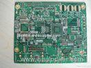
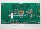
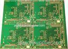
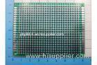
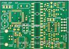
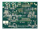
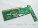
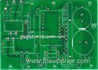
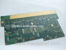
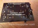
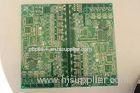
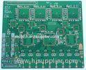
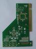
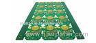
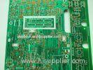
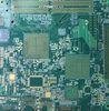
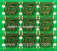
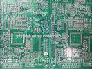
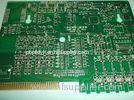
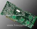
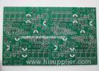
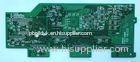
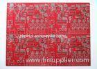
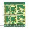
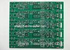
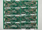
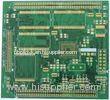
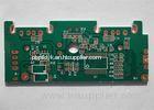
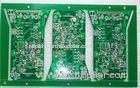
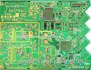
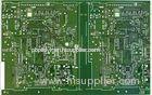
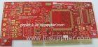
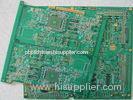
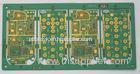
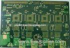
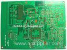
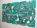
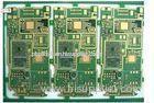
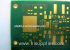
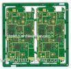
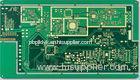
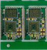
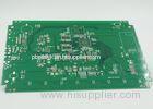
Fiducial Mark Added Double Sided PCB Gold Surface Plating PTH / NPTH Vias
| Place of Origin: | Zhejiang, China (Mainland) |
|
|
|
| Add to My Favorites | |
| HiSupplier Escrow |
Product Detail
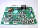
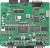
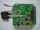
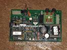
Fiducial Mark Added Double Sided PCB Gold Surface Plating PTH / NPTH Vias</p
Fiducial Mark Added Double Sided PCB Gold Surface Plating PTH / NPTH Vias
Advantage
1.PCB factory directly
2.PCB high quality
3.PCB good price
4.PCB quick time
5.PCB certification(ISO/UL E354810/RoHS)
Capability
|
High precision prototype |
PCB bulk production |
||
|
Max Layers |
1-28 layers |
1-14 layers |
|
|
MIN Line width(mil) |
3mil |
4mil |
|
|
MIN Line space(mil) |
3mil |
4mil |
|
|
Min via (mechanical drilling) |
Board thickness≤1.2mm |
0.15mm |
0.2mm |
|
Board thickness≤2.5mm |
0.2mm |
0.3mm |
|
|
Board thickness2.5mm |
Aspect Ration≤13:1 |
Aspect Ration≤13:1 |
|
|
Aspect Ration |
Aspect Ration≤13:1 |
Aspect Ration≤13:1 |
|
|
Board thickness |
MAX |
8mm |
7mm |
|
MIN |
2 layers:0.2mm;4 layers:0.35mm;6 layers:0.55mm;8 layers:0.7mm;10 layers:0.9mm |
2 layers:0.2mm;4 layers:0.4mm;6 layers:0.6mm;8layers:0.8mm |
|
|
MAX Board size |
610*1200mm |
610*1200mm |
|
|
Max copper thickness |
0.5-6oz |
0.5-6oz |
|
|
Immersion Gold/ Gold Plated Thickness |
Immersion Gold:Au,1—8u” |
||
|
Hole copper thick |
25um 1mil |
25um 1mil |
|
|
Tolerance |
Board thickness |
Board thickness≤1.0mm:+/-0.1mm |
Board thickness≤1.0mm:+/-0.1mm |
|
Outline Tolerance |
≤100mm:+/-0.1mm |
≤100mm:+/-0.13mm |
|
|
Impedance |
±10% |
±10% |
|
|
MIN Solder mask bridge |
0.08mm |
0.10mm |
|
|
Plugging Vias capability |
0.25mm--0.60mm |
0.70mm--1.00mm |
|
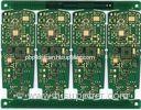
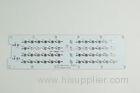
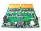
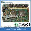
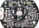
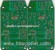
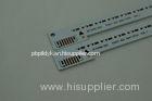
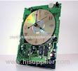
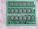
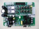
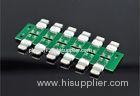
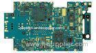
"2L PCB" has 2 copper trace, and also named as "Double Sided PCB" (D/S PCB). PTH (Via) is a must, but it still doesn't has Buried or Blind hole. Components can be assembled on both top and bottom side, so you don't need to worry about where to put components on the board, and not need to use through hole components which is always expensive than SMD one.

Related Search
Find more related products in following catalogs on Hisupplier.com
Company Info
China PCB Prototype Board Online Market [China (Mainland)]
Business Type:Manufacturer
City: Shenzhen
Province/State: Guangdong
Country/Region: China (Mainland)