|
China PCB Prototype Board Online Market
|
Gold Index: 12474


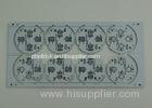
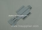
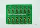
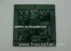
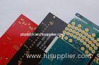
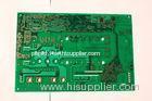
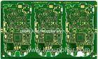
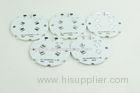
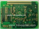
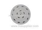
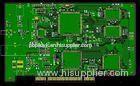
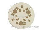
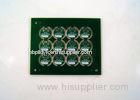
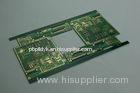
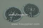
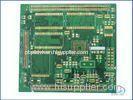
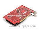
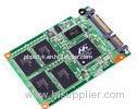
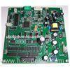
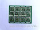
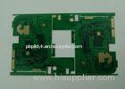
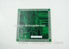
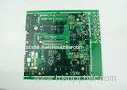
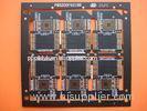
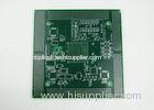
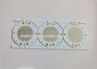
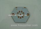
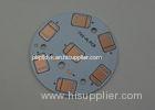
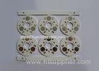
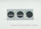
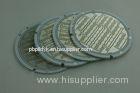
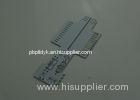
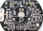
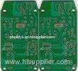
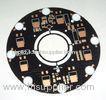
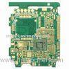
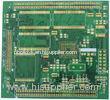
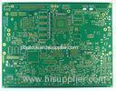
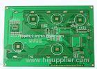
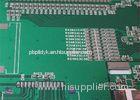
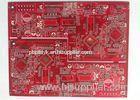
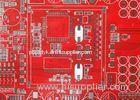
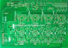
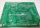
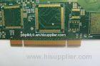
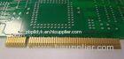
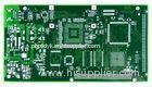
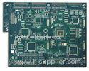
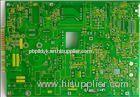
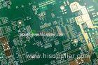
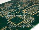
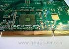
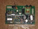
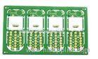
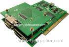
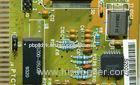
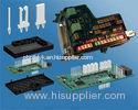
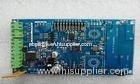
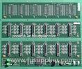
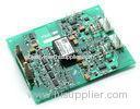
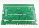
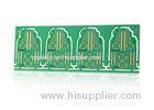
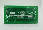
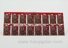
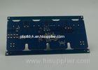
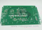
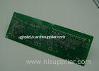
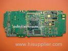
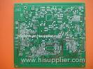
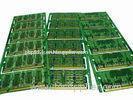
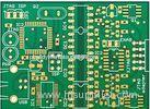
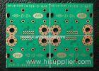
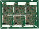
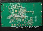
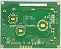
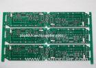
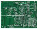
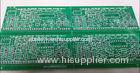
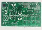
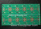
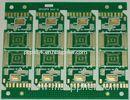
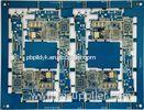
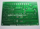
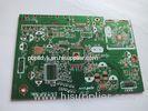
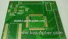
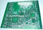
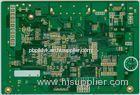
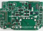
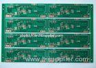
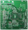
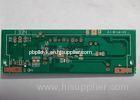
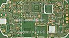
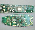
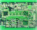
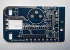
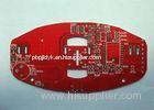
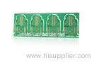
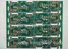
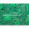
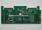
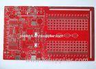
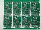
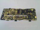
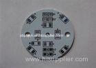
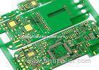
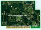
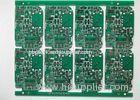
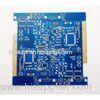
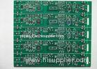
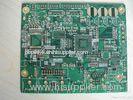
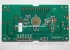
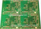
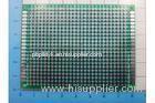
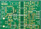
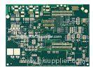
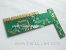
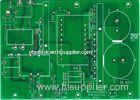
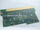
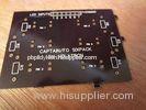
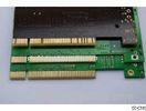
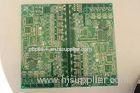
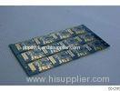
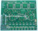
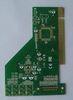
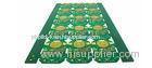
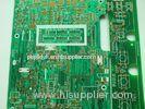
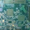
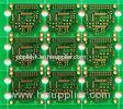
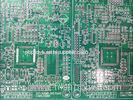
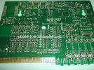
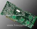
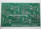
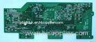
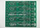
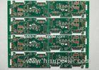
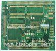
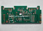
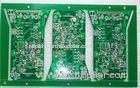
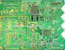
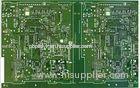
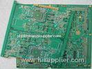
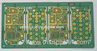
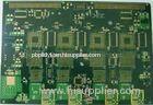
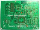
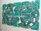
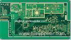
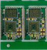
Custom PCB Boards HASL Double Layer PCB Green Solder Mask
| Place of Origin: | Zhejiang, China (Mainland) |
|
|
|
| Add to My Favorites | |
| HiSupplier Escrow |
Product Detail
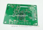
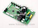
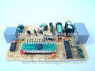
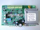
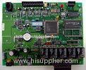
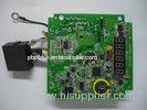
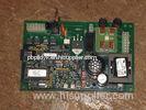
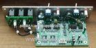
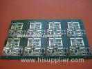
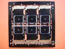
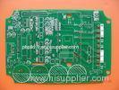
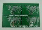
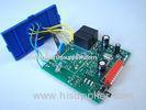
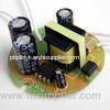
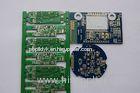
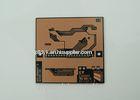
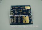
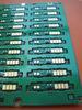
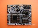
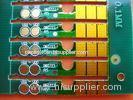
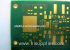
Custom PCB Boards HASL Double Layer PCB Green Solder Mask
<
Custom PCB Boards HASL Double Layer PCB Green Solder Mask
Quick Details
- Certifications of ISO9001:2008,UL,CE,ROHS,REACH,HALOGEN-FREE is meet.
- Best service with quick response is always provided for our customers.
- All kinds of surface finish is accepted,such as ENIG,OSP.Immersion Silver,Immersion Tin, Immersion Gold, Lead-free HASL,HAL.
- Advanced production equipment imported from Japan and Germany,such as PCB Lamination Machine, CNC drilling machine,Auto-PTH line, AOI(Automatic Optic Inspection),Probe Flying Machine and so on.
- BGA,Blind&Buried Vias and Impedence Control is accepted.
- Quality guarantee and professional after-sale service.
- Gerber file needed.
|
PRODUCT’S DETAILS |
|
|
Raw Material |
FR-4 (Tg 180 available) |
|
Layer Count |
4-Layer |
|
Board Thickness |
2.0mm |
|
Copper Thickness |
2.0oz |
|
Surface Finish |
ENIG(Electroless Nickel Immersion Gold) |
|
Solder Mask |
Green |
|
Silkscreen |
White |
|
Min. Trace Width/Spacing |
0.075/0.075mm |
|
Min. Hole Size |
0.25mm |
|
Hole Wall Copper Thickness |
≥20μm |
|
Measurement |
300×400mm |
|
Packaging |
Inner: Vacuum-packed in soft plastic bales |
|
Application |
Communication,automobile,cell,computer,medical |
|
Advantage |
Competitive Price,Fast Delivery,OEM&ODM,Free Samples, |
|
Special Requirements |
Buried And Blind Via, Impedance Control, Via Plug, |
|
Certification |
UL,ISO9001:2008,ROHS,REACH,SGS,HALOGEN-FREE |
|
PRODUCTION CAPABILITY OF PCB |
||
|
|
ITEMS Item |
|
|
Laminate |
Type |
FR-1,FR-5,FR-4 High-Tg,ROGERS,ISOLA,ITEQ, |
|
Thickness |
0.23.2mm |
|
|
Production Type |
Layer Count |
2L-16L |
|
Surface Treatment |
HAL,Gold Plating,Immersion Gold,OSP, |
|
|
Cut Lamination |
Max. Working Panel size |
1000×1200mm |
|
Inner Layer |
Internal Core Thickness |
0.12.0mm |
|
Internal width/spacing |
Min: 4/4mil |
|
|
Internal Copper Thickness |
1.0~3.0oz |
|
|
Dimension |
Board Thickness Tolerance |
±10% |
|
Interlayer Alignment |
±3mil |
|
|
Drilling |
Manufacture Panel Size |
Max: 650×560mm |
|
Drilling Diameter |
0.25mm |
|
|
Hole Diameter Tolerance |
±0.05mm |
|
|
Hole Position Tolerance |
±0.076mm |
|
|
Min.Annular Ring |
0.05mm |
|
|
PTH+Panel Plating |
Hole Wall copper Thickness |
20um |
|
Uniformity |
90% |
|
|
Outer Layer |
Track Width |
Min: 0.08mm |
|
Track Spacing |
Min: 0.08mm |
|
|
Pattern Plating |
Finished Copper Thickness |
1oz3oz |
|
EING/Flash Gold |
Nickel Thickness |
Related Search
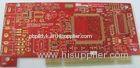
Red Solder Mask Pcb
Double Layer Pcb
Fr4 Pcb White Solder
10 Layer Pcb
6 Layer Pcb
4 Layer Pcb
More>>
Find more related products in following catalogs on Hisupplier.comRelated Products
Company InfoChina PCB Prototype Board Online Market [China (Mainland)]
Business Type:Manufacturer You May Like:
Printable Page
Bookmark this page
Sitemap XML About HiSupplier Help Center Customer Service Friend Links Site Map Archives Browse by: China Suppliers - Hot Products - Products Directory - Offers Directory - Suppliers Directory - Buyers Directory Language Option: العربية - Nederlands- Français- Deutsch- Italiano- 日本語- 한국의- Português- Pусский- Español Copyright © HiSupplier.com Online Inc. All Rights Reserved.

|