|
China PCB Prototype Board Online Market
|
Gold Index: 12474


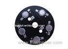
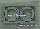
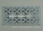
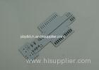
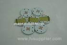
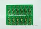
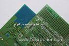
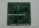
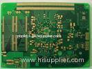
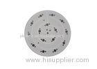
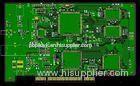
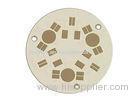
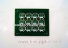
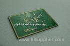
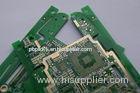
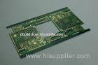
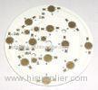
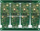
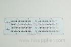
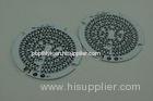
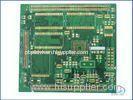
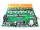
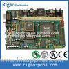
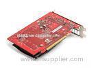
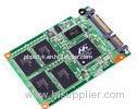
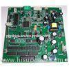
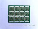
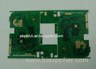
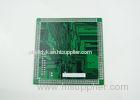
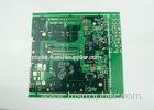
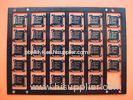
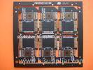
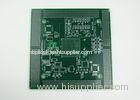
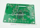
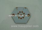
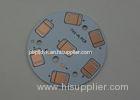
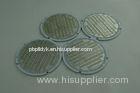
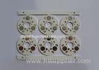
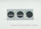
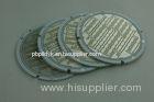
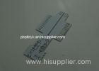
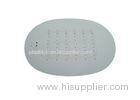
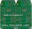
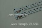
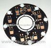
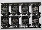
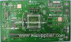
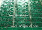
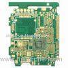
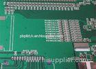
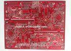
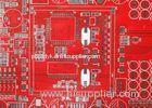
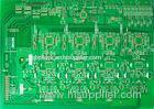
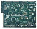
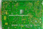
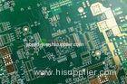
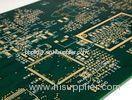
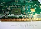
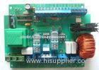
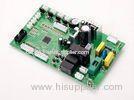
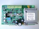
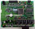
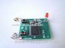
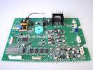
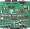
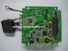
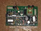
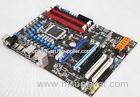
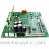
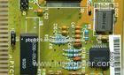
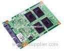
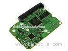
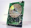
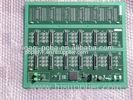
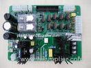
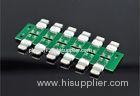
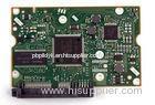
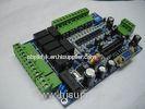
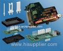
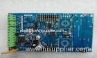
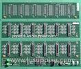
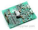
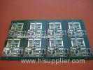
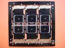
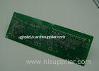
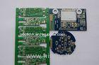
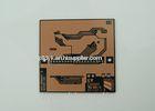
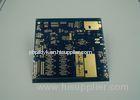
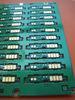
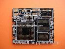
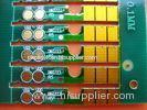
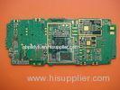
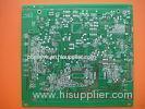
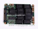
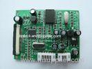
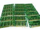
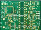
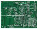
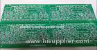
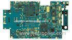
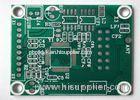
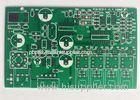
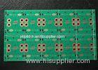
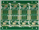
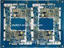
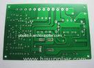
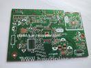
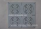
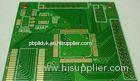
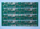
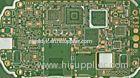
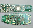
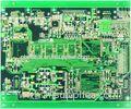
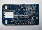
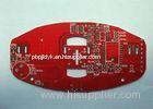
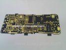
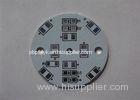
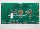
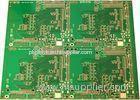
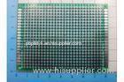
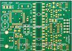
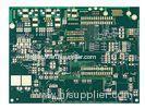
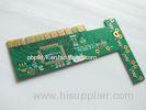
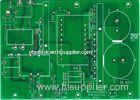
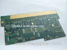
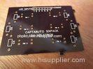
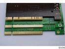
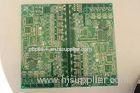
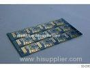
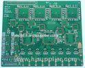
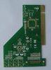
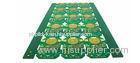
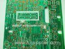
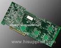
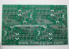
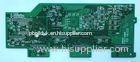
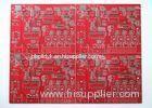
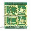
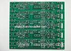
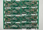
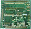
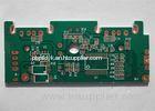
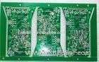
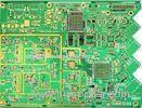
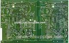
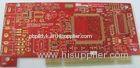
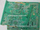
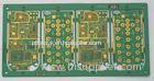
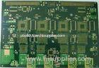
ODM FR4 PCB Printed Circuit Board for Power bank SMD Products
| Place of Origin: | Zhejiang, China (Mainland) |
|
|
|
| Add to My Favorites | |
| HiSupplier Escrow |
Product Detail
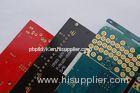
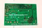
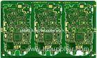
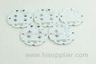
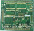
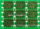
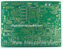
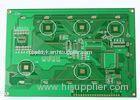
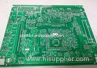
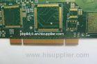
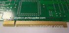
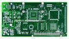
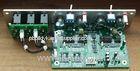
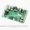
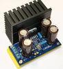
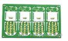
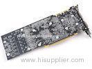
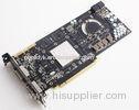
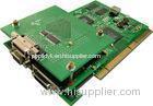
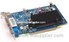
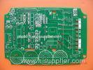
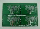
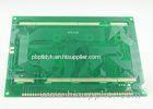
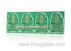
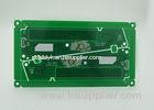
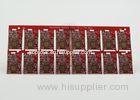
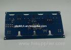
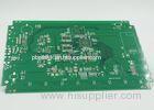
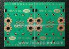
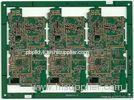
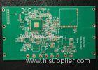
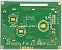
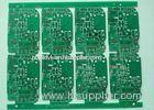
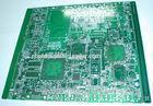
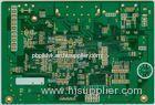
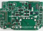
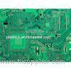
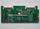
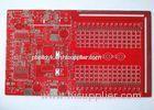
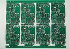
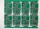
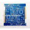
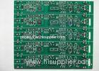
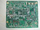
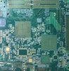
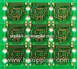
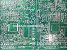
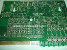
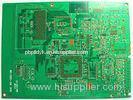
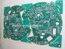
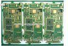
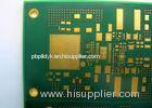
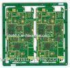
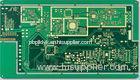
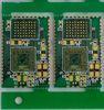
ODM FR4 PCB Printed Circuit Board for Power bank SMD Products<
ODM FR4 PCB Printed Circuit Board for Power bank SMD Products
Quick Details:
- Quality guarantee and professional after-sale service.
- PCBA,OEM,ODM service are provided.
- Professional PCB manufacturer.
- Gerber file needed.
|
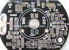
Printed Circuit Board DETAILS |
|
|
Raw Material |
FR4 based material |
|
Board Thickness |
2.0 mm |
|
Layer Count |
4-Layer |
|
Copper Thickness |
1.0 oz |
|
Surface Finish |
Immerssion Tin |
|
Solder Mask |
Green |
|
Silkscreen |
White |
|
Min. Trace Spacing |
0.045/0.045mm |
|
Min. Hole Size |
0.25mm |
|
Hole Copper Thickness |
≥20μm |
|
Measurement |
18×42mm |
|
Packing |
Outer: Cardboard Cartons with double straps Inner: Vacuum-packed in soft plastic bales |
|
Certificates |
HALOGEN-FREE,UL,ISO9001:2008,ROHS,REACH,SGS |
|
Advantage |
OEM&ODM,Competitive Price,Fast Delivery,Free Samples, |
|
Special Requirements |
Buried And Blind Via, Impedance Control, Via Plug, |
|
Applications |
Communication,automobile,cell,computer,medical |
|
CAPABILITY OF PRODUCTS |
||
|
Engineer Process |
Items |
Production Capability |
|
Laminate Board |
Thickness |
0.23.2mm |
|
Product Type |
Layer Count |
2L-16L |
|
Cut Lamination |
Max. Working Panel size |
1000×1200mm |
|
Inner Layer |
Core Thickness inside |
0.12.0mm |
|
Internal spacing |
Min: 4/4mil |
|
|
Internal Copper Thickness |
1.0~3.0oz |
|
|
Tolerance |
Tolerance Board Thickness |
±10% |
|
Inter layer Alignment |
±3mil |
|
|
Drilling |
Manufacture Panel Size |
Max: 650×560mm |
|
Drilling Diameter |
0.25mm |
|
|
Hole Diameter Tolerance |
±0.05mm |
|
|
Hole Position Tolerance |
±0.076mm |
|
|
Min.Annular Ring |
0.05mm |
|
|
PTH+Panel Plating |
Hole Wall copper Thickness |
20um |
|
Uniformity |
90% |
|
|
Outer Layer |
Track Width |
Min: 0.08mm |
|
Track Spacing |
Min: 0.08mm |
|
|
Pattern Plating |
Finished Copper Thickness |
1oz3oz |
|
EING/Flash Gold |
Related Search
Printed Circuit Board
Rigid Printed Circuit Board
Printed Circuit Board Assembly
Flexible Printed Circuit Board
Multilayer Printed Circuit Board
Hdi Printed Circuit Board
More>>
Find more related products in following catalogs on Hisupplier.com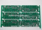
Company InfoChina PCB Prototype Board Online Market [China (Mainland)]
Business Type:Manufacturer You May Like:
Printable Page
Bookmark this page
Sitemap XML About HiSupplier Help Center Customer Service Friend Links Site Map Archives Browse by: China Suppliers - Hot Products - Products Directory - Offers Directory - Suppliers Directory - Buyers Directory Language Option: العربية - Nederlands- Français- Deutsch- Italiano- 日本語- 한국의- Português- Pусский- Español Copyright © HiSupplier.com Online Inc. All Rights Reserved.

| |